Lathrop had spent years looking through microscopes to make something small look bigger. As he puzzled over how to miniaturize transistors, he and Nall wondered whether microscope optics turned upside down could let something big—a pattern for a transistor—be miniaturized. To find out, they covered a piece of germanium material with a type of chemical called a photoresist, which they acquired from Eastman Kodak, the camera company. Light reacts with photoresist, making it either harder or weaker. Lathrop took advantage of this feature and created a “mask” in the shape of a mesa, placing it on the microscope with upside-down optics. Light that passed through holes in the mask was shrunk by the microscope’s lens and projected onto the photoresist chemicals. Where the light struck, the chemicals hardened. Where light was blocked by the mask, they could be washed away, leaving a precise, miniature mesa of germanium. A way to manufacture miniaturized transistors had been found.
Lathrop named the process photolithography—printing with light—and he and Nall filed for a patent. They delivered a paper on the topic at the annual International Electron Devices Meeting in 1957, and the Army awarded him a $25,000 prize for the invention. Lathrop bought his family a new station wagon with the money.
In the midst of the Cold War, the market for mortar fuzes was growing, but Lathrop’s lithography process took off because companies producing transistors for civilian electronics realized its transformative potential. Lithography not only produced transistors with unprecedented precision but also opened the door to further miniaturization. The two companies leading the race to commercial transistors—Fairchild Semiconductor and Texas Instruments—understood the implications early on. Lithography was the tool they needed to manufacture transistors by the millions, turning them into a mass-market good.
Painting with light
Robert Noyce, one of the cofounders of Fairchild, had studied alongside Lathrop when both had been PhD students in physics at MIT. The two of them had spent their weekends in graduate school hiking New Hampshire’s mountains, and they had stayed in touch after graduating. At Fairchild, Noyce moved quickly to hire Nall, Lathrop’s lab partner, and spearheaded his company’s lithography efforts by jury-rigging his own device with a set of 20-millimeter camera lenses he’d bought from a Bay Area photography shop.
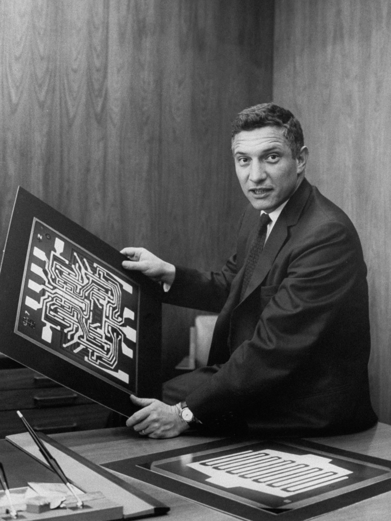
Lathrop, meanwhile, took a job at Fairchild’s competitor, Texas Instruments, driving his new station wagon down to Dallas. He arrived just as his new colleague and lifelong friend Jack Kilby was on the brink of creating a piece of semiconductor material with multiple electronic components built—or integrated—into it. These integrated circuits, it soon became clear, could be efficiently produced only with Lathrop’s lithography method. As chip firms strove to shrink transistors to cram more of them onto chips, photolithography provided the precision that miniaturized manufacturing required.
Fairchild and Texas Instruments made their first lithography machines in house, but the growing complexity of the machines soon attracted new entrants. As the scale of transistors declined from centimeters to millimeters to microns, the importance of precision optics increased. Perkin-Elmer was a Connecticut-based firm that produced specialized optics for the US military, from bombsights to spy satellites. In the late 1960s, it realized that this expertise could be used for lithography, too. It developed a scanner that could project the mask pattern onto a silicon wafer while aligning them with almost flawless precision. The scanner then moved a light across the wafer like a copy machine, painting it with lines of light. This tool proved capable of fabricating transistors as small as a micron—one millionth of a meter.
TED STRESHINSKY/GETTY IMAGES
But the approach wasn’t practical as chip features got still smaller. By the late 1970s, scanners began to be replaced with steppers, machines that moved light in discrete steps across a wafer. The challenge with a stepper was to move the light with micron-scale precision, so that each flash was perfectly aligned with the chip. GCA, a Boston-based firm that had its origins in spy balloons, devised the first stepper tool, reportedly on the advice of Texas Instruments executive Morris Chang—later the founder of TSMC, which is today the world’s largest chipmaker.
New England’s specialist lithography firms soon faced steep competition. In the 1980s, as Japanese chipmakers began winning major market share in the production of memory chips, they started buying from Nikon and Canon, two homegrown producers of lithography tools. Around the same time, the Dutch chipmaker Philips spun out its own unit that made lithography tools, calling the new company ASML.